NVT210
http://onsemi.com
4
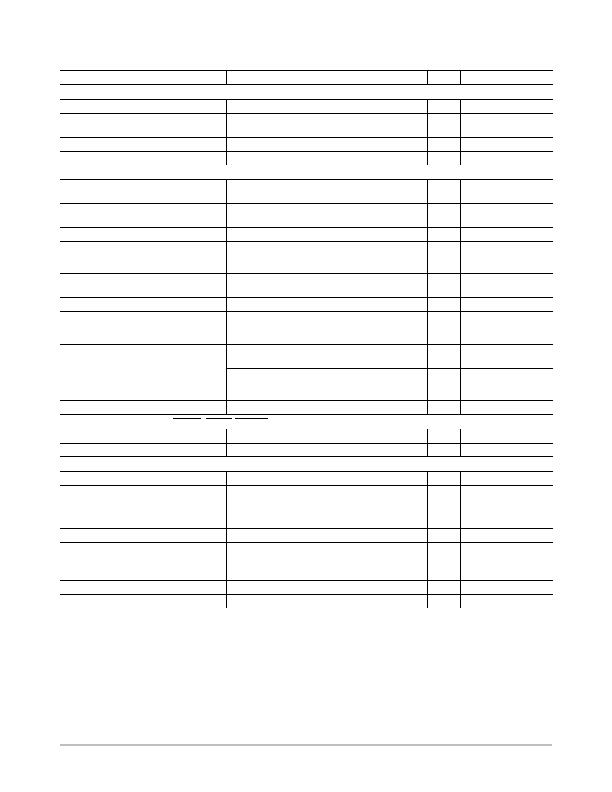
Table 5. ELECTRICAL CHARACTERISTICS (T
A
= 40癈 to +125癈, V
DD
= 2.8 V to 3.6 V, unless otherwise noted)
Parameter
Conditions
Min
Typ
Max
Unit
Power Supply
Supply Voltage, V
DD
2.8
3.30
3.6
V
Average Operating Supply Current, I
DD
0.0625 Conversions/Sec Rate (Note 1, 2)
Standby Mode
240
5.0
350
30
mA
Undervoltage Lockout Threshold
V
DD
input, disables ADC, rising edge
2.55
V
Power-on Reset Threshold
1.0
2.56
V
Temperature-to-Digital Converter
Local Sensor Accuracy
3.0 V to 3.6 V
0癈 ?T
A
?+70癈
0癈 ?T
A
?+85癈
?.0
?.5
癈
Local Sensor Accuracy
2.8 V to 3.6 V
20癈 ?T
A
?+110癈
?.5
癈
Resolution
1.0
癈
Remote Diode Sensor Accuracy
3.0 V to 3.6 V
0癈 ?T
A
?+70癈, 55癈 ?T
D
(Note 3) ?+150癈
0癈 ?T
A
?+85癈, 55癈 ?T
D
(Note 3) ?+150癈
40癈 ?T
A
?+100癈, 55癈 ?T
D
(Note 3) ?+150癈
?.0
?.5
?.5
癈
Remote Diode Sensor Accuracy
2.8 V to 3.6 V
0癈 ?T
A
?+70癈, 20癈 ?T
D
?+110癈
20癈 ?T
A
?+110癈, T
D
= +40癈
?.5
?.25
癈
Resolution
0.25
癈
Remote Sensor Source Current
High Level (Note 3)
Middle Level (Note 3)
Low Level (Note 3)
220
82
13.5
mA
Conversion Time
From Stop Bit to Conversion Complete, One-shot
Mode with Averaging Switched On
40
52
ms
One-shot Mode with Averaging Off
(that is, Conversion Rate = 16-, 32-, or
64-conversions per Second)
6.0
8.0
ms
Maximum Series Resistance Cancelled
Resistance Split Evenly on both the D+ and D Inputs
1.5
kW
Open-drain Digital Outputs (THERM
, ALERT
/THERM2
)
Output Low Voltage, V
OL
I
OUT
= 6.0 mA
0.4
V
High Level Output Leakage Current, I
OH
V
OUT
= V
DD
0.1
1.0
mA
SMBus/I
2
C Interface (Note 4 and 5)
Logic Input High Voltage, V
IH
SCLK, SDATA
1.4
V
Logic Input Low Voltage, V
IL
SCLK, SDATA
0.8
V
Hysteresis
500
mV
SDA Output Low Voltage, V
OL
0.4
mA
Logic Input Current, I
IH
, I
IL
1.0
+1.0
mA
SMBus/I
2
C Input Capacitance,
SCLK, SDATA
5.0
pF
SMBus/I
2
C Clock Frequency
400
kHz
SMBus/I
2
C Timeout (Note 6)
User Programmable
25
64
ms
SCLK Falling Edge to SDATA Valid Time
Master Clocking in Data
1.0
ms
1. See Table 9 for information on other conversion rates.
2. THERM
and ALERT
pulled to V
DD
.
3. Guaranteed by characterization, but not production tested.
4. Guaranteed by design, but not production tested.
5. See SMBus/I
2
C Timing Specifications section for more information.
6. Disabled by default. Detailed procedures to enable it are in the Serial Bus Interface section of the datasheet.
发布紧急采购,3分钟左右您将得到回复。
相关PDF资料
PI5L102LE
IC HOT SWAP PULL-UP SW 20-TSSOP
QPI-8LZ-01
IC HOT SWAP EMI FILTER 16LGA
SA56004HD,118
IC TEMP SENSOR DIGITAL 8SOIC
SC2463TSTRT
IC REG QD BCK/LINEAR 28TSSOP
SC338AIMSTRT
IC REG CTRLR DUAL POS ADJ 10MSOP
SC402BMLTRT
IC REG DL BCK/LINEAR SYNC 32MLPQ
SC403MLTRT
IC REG DL BCK/LINEAR SYNC 32MLPQ
SC418ULTRT
IC REG DL BUCK/LINEAR 20MLPQ
相关代理商/技术参数
NVT-3402
制造商:Quest Technology International Inc 功能描述:
NVT-3403
制造商:Quest Technology International Inc 功能描述:
NVT4555UKZ
功能描述:SIM Card Interface 12-WLCSP (1.20x1.60) 制造商:nxp semiconductors 系列:- 包装:剪切带(CT) 零件状态:停产 应用:SIM 卡 接口:- 电压 - 电源:1.1 V ~ 3.6 V 封装/外壳:12-UFBGA 供应商器件封装:12-WLCSP(1.20x1.60) 安装类型:表面贴装 标准包装:1
NVT4556AUKZ
功能描述:SIM Card Interface 12-WLCSP (1.20x1.60) 制造商:nxp semiconductors 系列:- 包装:剪切带(CT) 零件状态:有效 应用:SIM 卡 接口:I2C 电压 - 电源:1.55 V ~ 3.6 V 封装/外壳:12-XFBGA 供应商器件封装:12-WLCSP(1.20x1.60) 安装类型:表面贴装 标准包装:1
NVT4556BUKZ
功能描述:SIM Card Interface 12-WLCSP (1.20x1.60) 制造商:nxp semiconductors 系列:- 包装:剪切带(CT) 零件状态:有效 应用:SIM 卡 接口:I2C 电压 - 电源:1.55 V ~ 3.6 V 封装/外壳:12-XFBGA 供应商器件封装:12-WLCSP(1.20x1.60) 安装类型:表面贴装 标准包装:1
NVTA7002NT1G
功能描述:MOSFET NFET SC75 30V 154MA 7OHM RoHS:否 制造商:STMicroelectronics 晶体管极性:N-Channel 汲极/源极击穿电压:650 V 闸/源击穿电压:25 V 漏极连续电流:130 A 电阻汲极/源极 RDS(导通):0.014 Ohms 配置:Single 最大工作温度: 安装风格:Through Hole 封装 / 箱体:Max247 封装:Tube
NV-TC20P
制造商:Panasonic Industrial Company 功能描述:DISCD TAPE
NV-TC30AH
制造商:Panasonic Industrial Company 功能描述:TAPE
